Syrma SGS

Blog Articles

PCBA vs Box Build: Key Differences and How to Choose

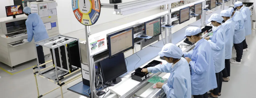
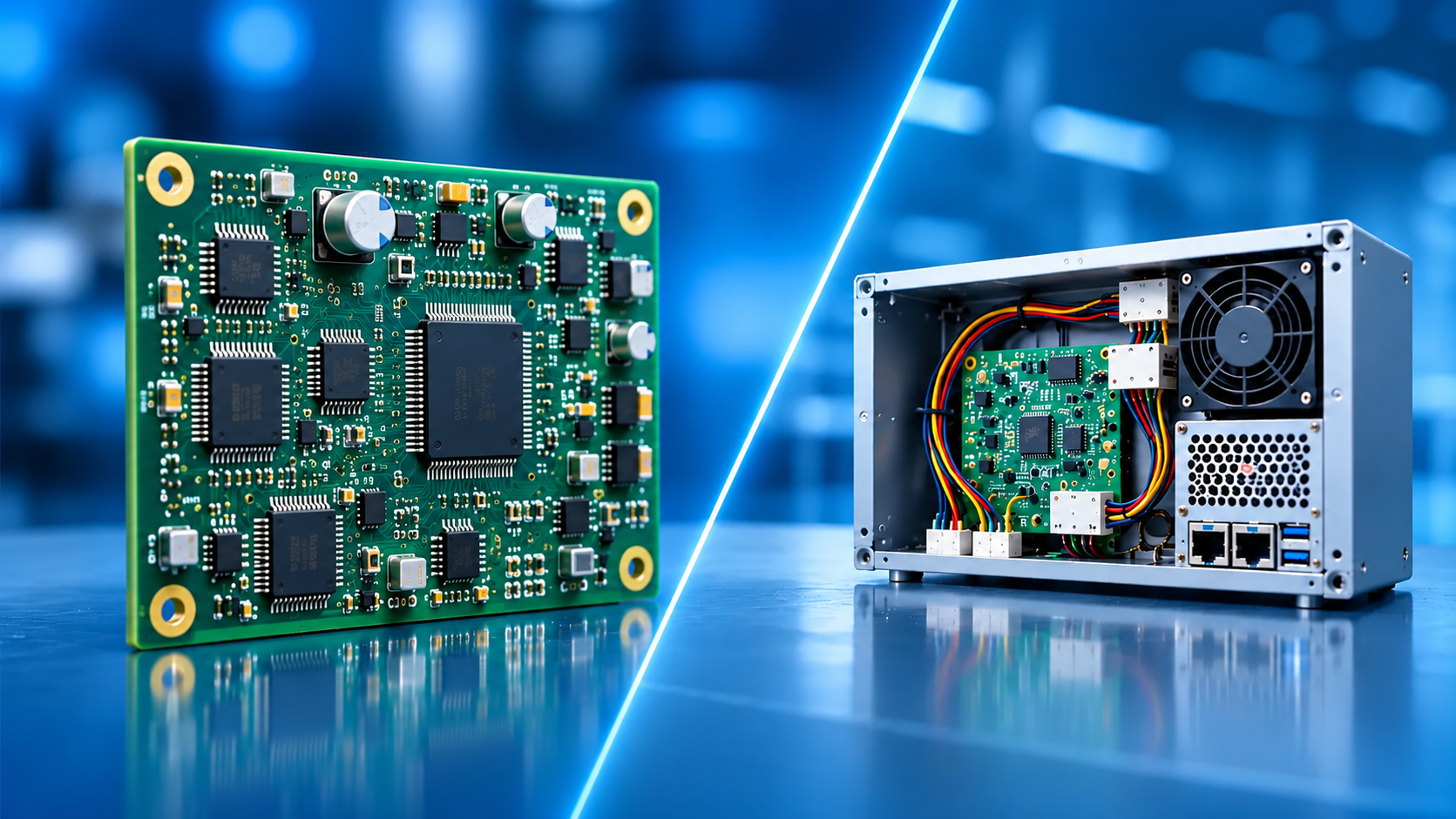
When a Circuit Board Needs to Become a Complete Product Electronic manufacturing extends beyond assembling components onto a printed circuit board (PCB). While printed circuit board assembly (PCBA) establishes the circuit’s electrical functionality, a complete product may also require enclosures, cables, wire harnesses, connectors and power supplies. Integrating these elements creates a functional electronic unit. Understanding the difference between PCBA and box build helps original equipment manufacturers (OEMs) define manufacturing requirements and allocate responsibilities effectively.  While PCBA focuses on board-level assembly, box build involves product integration and system-level testing. The right choice depends on product complexity, in-house capabilities, testing requirements and the intended deliverable.   PCBA vs Box Build: The Difference at a Glance PCBA focuses on assembling electronic components onto a printed circuit board, while box build integrates the assembled board with mechanical and electrical components to create a functional product.  Understanding the difference helps OEMs define manufacturing scope, testing requirements and final deliverables based on product complexity. Comparison Factor PCBA Manufacturing Box Build Assembly Primary purpose Assembles electronic components onto a printed circuit board (PCB). Integrates PCBAs with mechanical and electrical components to create a functional subassembly or complete product. Manufacturing activities Solder paste application, component placement, soldering, inspection and board assembly. PCBA installation, enclosure assembly, wiring, cable integration and mechanical and electrical integration. Components involved Bare PCBs, integrated circuits, resistors, capacitors and electronic connectors. PCBAs, enclosures, cables, wire harnesses, power supplies, switches, cooling fans and mounting hardware. Testing requirements Automated optical inspection (AOI), X-ray inspection where required, in-circuit testing and board-level functional testing. Continuity checks, interconnection verification, system-level functional testing and end-of-line testing, as specified. Final deliverable An assembled circuit board that meets the agreed manufacturing and testing requirements. An integrated electronic subassembly or finished product, depending on the agreed manufacturing scope. Typical applications Control boards, power supply boards, communication modules and embedded electronic circuits. Industrial controllers, power electronics units, communication equipment and electronic devices. Best suited for OEMs with in-house capabilities for enclosure assembly, wiring and final product integration. OEMs seeking a broader manufacturing solution that integrates electronic, mechanical and electrical components. Key advantage Enables focused, precise circuit-board assembly and board-level quality control. Consolidates multiple assembly stages and supports streamlined product integration. PCBA focuses on circuit-board assembly, while box build extends manufacturing to product-level integration.  The appropriate option depends on product complexity, internal manufacturing capabilities, testing requirements and the final deliverable expected from the EMS provider. What Does PCBA Manufacturing Include? PCBA manufacturing involves attaching and soldering electronic parts to a blank PCB to produce a working circuit board.  Accurate component placement, soldering control, and defect identification through quality checks ensure your final product meets the drawings and performance requirements. Below are the major phases in PCBA manufacturing: Solder paste printing: The method here is to place the solder paste (a mixture of solder and flux) onto specific pads of the PCB via a printed stencil. Precisely applied solder paste forms solid electrical and mechanical bonds during the soldering process. Component placement: In this step, a fully automatic pick-and-place machine places surface-mount components like resistors, capacitors, or integrated circuits on the PC board design, also in accordance with the bill of materials (BOM). On the other hand, through-hole components can be mounted separately if there is a need. Soldering: The soldering of a surface-mount component is done mostly via reflow soldering. Through-hole components, on the other hand, can be soldered using wave, selective, or hand soldering, depending on the design of the board and the specifications of the component. Inspection and Quality Control: A combination of inspection techniques such as automated optical inspection (AOI), X-ray inspection and others serve as a means to detect component misalignment, soldering defects besides hidden joint issues if there are any. Board-level test: According to the product specifications, after assembly, the boards may be subjected to in-circuit (ICT) or functional test to verify electrical connections and operational functionality. The manufacturing procedure is not only affected by the complexity and component types but also by application requirements.  A properly controlled PCBA procedure will enable consistent assembly, product reliability and overall manufacturing quality before the board is integrated into a system or delivered as a separate ​‍​‌‍​‍‌assembly. What Does Box Build Assembly Include? Box build assembly is basically putting together a piece of electronics by connecting together PCBs with other mechanical, electrical and electromechanical components.  The process consists of several major parts such as:   Enclosure & Mechanical Assembly The main function of the enclosure is to house all other components and to protect them while simultaneously providing structure to the whole package. It is also crucial that components are placed properly so that they do not come into unintended contact or interference. Assembly of the enclosure and parts such as brackets and hardware is what gives you the structure. PCBA Integration PCBs that have been built are then placed into the enclosure using mounting arrangements specified for the component. Also, the clearance, electrical isolation and heat aspects are taken care of properly. Cable and Wire Harness Installation Installation of cable, wiring harness and connectors is the means of achieving all required electrical communications (i.e., signal and power delivery) through PCBs – power supply units, sensors, displays, interfaces external (e.g., USB port). Component Integration Depending on the requirements of the product, other necessary parts, such as cooling fans, sensors, switches, power supply units and communication modules, were fitted to the device. Functional Testing and Quality Inspection Upon completion of the assembly and packaging, the product is subjected to various quality control tests, such as insulation test, continuity check and functional test, so as to guarantee system performance and correct interfacing. Final Inspection Labeling, configuration checking, documentation and packing are fully completed under the requirements of the agreed-upon manufacturing ​‍​‌‍​‍‌process. Where Does PCBA End and Box Build Begin? The line between PCBA work and box build depends on a manufacturing agreement between the OEM and its electronics manufacturing services (EMS) provider. PCBA – Board-Level Assembly One of the major processes of PCBA is the

PCBA vs Box Build: Key Differences and How to Choose Read More »

RFID with AI for Food Safety: How Smarter Systems Reduce Risk

The Invisible Gaps: How Risks Build Across the Food Supply Chain   Food safety is no longer just a matter of periodic inspections and manual logs. In today’s globalized supply chains, risks can emerge silently across storage facilities, transport routes, and distribution networks long before a product reaches the consumer. As food systems become more complex, technologies like RFID and Artificial Intelligence (AI) are transforming how safety is monitored, predicted and enforced. At Syrma SGS, where precision manufacturing meets scalable electronics solutions, we see this shift as foundational: food safety is moving from reactive control to intelligent prevention. Beneath the Surface: What Powers RFID and AI in Food Safety Systems Maintaining food safety throughout today’s supply chains is not just about occasional inspections and manual record-keeping. RFID and AI come together to build a smart monitoring setup that offers continuous visibility, traceability and actionable insights at each stage of the product life cycle.   RFID Tags Enable Product Identification: RFID tags attached to food items, pallets, or containers provide unique identification data, allowing products to be tracked accurately from production to delivery. Sensors Capture Critical Environmental Conditions: Connected sensors can continuously monitor temperature, humidity, shock and other factors that directly impact food quality and safety. RFID Readers Collect Real-Time Data: Installed at warehouses, transportation hubs and distribution centers, RFID readers automatically capture information from tagged products without manual intervention. Cloud Platforms Centralize Information: Data collected from RFID devices and sensors is transmitted to cloud-based systems, creating a single source of truth accessible across the supply chain. AI Transforms Data into Insights: Artificial Intelligence analyzes large volumes of real-time and historical data to identify patterns, detect anomalies and evaluate potential risks. Improved Decision-Making Across Operations: By combining RFID-generated visibility with AI-driven analytics, businesses can respond faster to temperature excursions, inventory issues and potential food safety concerns before they escalate. In fact, together, RFID and AI help form a connected food safety system that improves traceability, strengthens regulatory adherence and assists with proactive risk management across the entire supply chain.   Turning Signals into Action: How Intelligence Starts Driving Decisions AI truly unlocks the power of RFID for food safety by converting the constant data streams into actionable insights. With RFID tags and connected sensors, a considerable amount of real-time data is generated on product location, temperature, humidity, and handling conditions throughout the entire supply chain. AI-driven analytics tools are able to process this data right away and detect patterns and anomalies that suggest potential risks. In this context, AI can identify temperature excursions that threaten cold-chain integrity, detect shipment delays that could increase spoilage risk, and flag environmental conditions that may contribute to contamination.   Instead of conducting inspections at intervals or resorting to manual interventions, companies are given real-time alerts, allowing them to take corrective action quickly and thus prevent deterioration of product quality. On top of that, AI constantly updates itself based on past and present data, becoming better at guiding decisions. Through this, food manufacturers, distributors and retailers get the opportunity to act even before a potential safety issue becomes a real problem, reduce waste, stay compliant with the regulations and keep consumers’ trust.  This leads to a smarter, more agile, and lasting food safety ​‍​‌‍​‍‌system. The Reality Check: Why Food Safety Still Breaks Despite Systems Food safety incidents can still occur worldwide at various points in the supply chain despite investments in monitoring technologies and quality control processes. Often, the problem is not that there are no systems but the operational gaps that prevent such systems from providing visibility and timely intervention.  As food products are transferred from one storage, transportation, and distribution stage, even minor disruptions are capable of posing significant safety risks.   Human Error Remains a Major Risk: Manual data entry, missed inspections, improper handling, and inconsistent record-keeping can introduce inaccuracies that compromise food safety and product quality. Limited Traceability Across Operations: Many organizations still operate with disconnected systems, making it difficult to track products seamlessly from production to consumption and quickly identify affected batches during an incident. Delayed Detection of Problems: Traditional monitoring methods often rely on periodic checks rather than continuous visibility, allowing spoilage, contamination, or temperature deviations to go unnoticed until products are already compromised. Increasing Compliance Pressure: Food manufacturers and distributors must comply with evolving regulatory requirements, requiring accurate documentation, traceability, and audit readiness across the entire supply chain. Maintaining Cold Chain Integrity: Temperature-sensitive products are vulnerable to storage and transportation fluctuations. Even brief temperature excursions can impact product safety, shelf life, and regulatory compliance. To overcome the above issues, implementing real-time visibility, automated monitoring, and intelligent decision-making capabilities is necessary because that way, the amount of human intervention is minimized and faster corrective actions can be ​‍​‌‍​‍‌taken.   Beyond Monitoring: When Systems Begin to Anticipate Risks The real value of integrating RFID with AI is not just about tracking the food products, but more so about identifying risks even before they have a chance to affect quality and safety.  Traditional food safety practices mainly detect problems post-factum, which often leads to product wastage, disruption of operations, and expensive recalls. Thanks to predictive AI, the whole scenario has transformed into an ongoing process of analysis of various data from RFID, such as temperature records, transit conditions, storage time, and inventory movement patterns, etc. Through pattern and deviation recognition, AI can identify the potential for goods to spoil but also estimate remaining shelf life and alert operators so they can take timely action before the decline in quality.  This way, companies can carry out actions like shipment rerouting, inventory rotation optimization, and adjusting storage conditions. Thus, waste is drastically minimized, freshness is maintained, and overall supply chain effectiveness is enhanced. Above all, prediction-driven data enables enterprises to reduce the risk of contamination incidents and large-scale product recalls, endangering customers and damaging brands. Indirectly, the food safety system evolves into a smarter one where risk control is largely preventative instead of being a reactive approach ​‍​‌‍​‍‌one. Testing Before Trust: Ensuring Reliability in

RFID with AI for Food Safety: How Smarter Systems Reduce Risk Read More »

Ferrite Core vs Iron Core Transformers: Which Is Better for Modern Electronics?

Two Transformers Can Look Similar: Their Core Choices Can’t   Two transformers may perform the same fundamental function transferring electrical energy and providing voltage transformation or isolation yet deliver very different performance. The key difference often lies in the magnetic core. A transformer designed for 50/60 Hz power conversion may use a laminated iron or silicon steel core. In contrast, a high-frequency transformer in an SMPS or DC-DC converter typically relies on ferrite. Core material influences how the transformer responds to operating frequency, magnetic flux, power levels and heat generation. It also affects physical size, weight, efficiency and allowable operating conditions. Therefore, transformer selection is not simply about voltage and power ratings; it requires matching the core technology to the application’s frequency, efficiency, thermal and space requirements.  Before Comparing Cores, Understand What the Core Does Choosing between ferrite and iron cores requires that you first understand the function of a transformer core. The core does not only serve as a structural element. Its role is a decisive factor in the extent and manner in which magnetic energy is shared between the windings and in the way the transformer handles different operating conditions. Provides a magnetic flux path: The core serves as a medium and guide for the magnetic flux from the winding to the core; as such, the coupling of the coils is enhanced. Influences energy transfer: Core permeability, size, and shape of the magnetic path can determine to a great extent the levels of magnetizing current, energy losses and power transmission capabilities through the transformer. Determines frequency capability: Properties of the core material, especially magnetic losses and electrical resistivity, dictate the frequencies at which a transformer can operate with minimum losses. Affects saturation: Each magnetic material has an upper bound for practical flux density. The magnetizing current and losses may increase greatly if the limits are exceeded. Impacts efficiency: Core losses in the form of hysteresis and eddy currents are major causes of heat generation and consequently reduction in overall efficiency of transformers. Influences transformer size: Characteristics of the core material, the operating frequency, magnetic path length/flux density and core shape are all factors that decide the volume of magnetic field necessary to reach a certain power  ‍ ‌‍ ‍‌level. Ferrite Core vs Iron Core: What Is the Real Difference? In transformer applications, “iron core” commonly refers to laminated electrical steel or silicon-steel cores, particularly for power-frequency transformers. Ferrite cores, by contrast, are ceramic magnetic materials based primarily on iron oxides combined with other metal oxides. Their different electrical and magnetic properties make them suitable for different operating conditions. Parameter Ferrite Core Laminated Iron/Steel Core Typical frequency range Medium to high frequency; widely used in kHz to MHz-range applications depending on material Primarily low-frequency applications, especially 50/60 Hz Electrical resistivity High Much lower Eddy-current losses at high frequency Relatively low Can become significant without specialized construction Saturation flux density Generally lower Generally higher Size at high frequency Compact Typically less suitable for high-frequency miniaturization Weight Lightweight Relatively heavy High-frequency efficiency Generally favorable Generally unfavorable as frequency rises Typical applications SMPS, DC-DC converters, high-frequency transformers, telecom power supplies Mains transformers, low-frequency power conversion, traditional industrial power systems Mechanical characteristics Ceramic and relatively brittle Stronger metallic construction Design priority High-frequency efficiency and power density Low-frequency power handling and high saturation capability This comparison does not mean that one material universally outperforms the other. It shows that each has a different performance window.  Where Ferrite Core Transformers Have the Advantage Ferrite core transformers are a major asset in modern power electronics where you have high switching frequencies, small component sizes and you want to transfer energy efficiently. Their material features provide quite significant improvements. High-frequency operation: Ferrite cores can very efficiently carry out their function when the frequency is very high, which makes them a perfect match for power converters that have to operate at such frequencies. Lower core losses: Their resistivity to the flow of electric charges decreases the eddy current losses even at high frequencies, thus leading to improved efficiency. Compact design: Transformers that operate at a higher frequency can reach the necessary energy levels with relatively smaller magnetic components. Lightweight construction: Smaller core and winding designs can reduce the overall weight of the transformer tremendously. Higher power density: It’s possible to use very compact ferrite transformers delivering very hefty power without needing much space, so it’s possible to have miniaturized designs. Better suitability for SMPS: Ferrite cores are the go-to option for switched-mode power supplies in which the fundamental requirement is high-frequency switching for reducing the size of components. DC-DC conversion: They can even be employed in isolated DC-DC converters on a wide scale in sectors that include industrial electronics, telecom systems, the car industry and other sectors that require power conversion. All things considered, the greatest benefit ferrite cores have is that they can combine high-frequency performance, efficiency, compact size and very good power density in just one magnetic ​‍​‌‍​‍‌component. Where Iron Core Transformers Work Best Steel or iron core laminations are still a good solution when it comes to transformers that operate at low frequency levels, especially for 50/60 Hz power conversion. A higher saturation flux density of the core means it can handle more magnetic flux before saturation sets in, which helps in maintaining a stable power transfer at mains frequencies. Besides, laminating the core is an effective method in diminishing eddy-current losses that can otherwise raise the level of heat generated and result in reduced efficiency. Although transformers made of steel or iron are more or less large and heavier than high-frequency ferrites, one may not always be after a compact and lightweight design. These transformers are the optimal solution for mains transformers, power distribution, isolation transformers and industrial power systems, where strong build quality, track record of performance and reliable low-frequency operation are valued over space-saving and lightness ​‍​‌‍​‍‌characteristics.  Ferrite vs Iron Core: Which One Handles Heat Better? Heat dissipation is primarily a design-dependent issue. Although one type of core may have advantages

Ferrite Core vs Iron Core Transformers: Which Is Better for Modern Electronics? Read More »

The Rise of Chipless RFID: What’s Driving It?

The First Crack in the System: When Tagging Costs Start Eating Margins   As supply chains become more complex, businesses are under increasing pressure to improve product visibility and inventory accuracy. Traditional RFID has helped address these demands by enabling automated tracking, but its cost can become difficult to justify in high-volume environments. For companies handling millions of low-cost items, adding a silicon-based RFID tag to every unit significantly increases overall operational expenses. Industries such as retail, packaging, logistics and FMCG operate on narrow margins, making cost efficiency essential. This challenge is driving businesses to explore more economical identification technologies that can maintain traceability while reducing tagging costs, making chipless RFID an increasingly relevant alternative. Beneath the Surface: Understanding What Chipless RFID Really Means Chipless RFID is an emerging approach to the identification and tracking technology space, one that eliminates the need for a silicon microchip that is a staple in the majority of RFID tags. Rather than having electronic memory as a medium for storing data, chipless RFID depends on engineered physical structures, conductive substances, resonant components, and uniquely arranged patterns to convey and encode information.   When stimulated by radio-frequency signals from a reader, these components produce distinct electromagnetic signals that can be captured and decoded to determine a product. Simply put, the data is “written” into the very makeup of the tag rather than electronically stored. This radically modified setup offers a significant benefit: fewer materials to work with, and thus reduced manufacturing costs. Doing away with the need for semiconductor parts, chipless RFID is a potential option for use in situations where a large number of units are required and traditional RFID is not very economically feasible. While it usually comes with a smaller amount of stored data compared to chip-based ones, chipless RFID still has the potential to make tracking simpler, lighter in weight, lower-cost identification and accessible to the industries that want more intelligent identification without increasing electronic ​‍​‌‍​‍‌​‍​‌‍​‍‌components. Scaling Struggles: How Traditional RFID Begins to Show Its Limits Traditional RFID has significantly improved inventory visibility and operational efficiency across industries. However, at high-volume scale in retail, packaging, and logistics, cost and material considerations can become more significant at very high volumes.  Rising Cost at Scale  At first glance, traditional RFID tags might look like simple devices, but they are actually more expensive than other identification methods because they consist of silicon chips and antenna assemblies. For companies that sell millions of low-cost products, quite small per-item costs add up fast and start affecting their overall profits. Durability Limitations in High-Throughput Environments The nature of RFID tags makes them susceptible to performance deterioration when exposed to packaging, handling, transport, or even environmental elements. Besides, they may suffer mechanical damage, or subjected to compression during packaging and transport could impact their reliability and consistent reading. Disposal and Sustainability Concerns  Because normal RFID contains electronic parts, disposal gets more complicated, especially in the case of single-use or disposable packaging. This poses difficulties for recycling and raises environmental concerns. Operational Complexity  Implementing large-scale operations also requires more infrastructure, integration, and frequent maintenance, thus increasing the overall deployment cost. All these pressure points for scaling are leading different sectors considering alternative identification technologies that provide traceability with less complexity and ​‍​‌‍​‍‌​‍​‌‍​‍‌cost. Quiet Adoption: The Spaces Where Chipless RFID Is Already Working Research initiatives, pilot projects, and early deployments are already exploring its practical applications. While chipless RFID is often positioned as an emerging technology, its adoption is beginning to take shape in sectors where high-volume identification, scalability and cost efficiency are becoming increasingly important.  By discarding the silicon chip and radically changing tag architecture, chipless RFID is opening the door for affordable, scaled-up tracking solutions in sectors where the use of traditional RFID is not always feasible from an economic standpoint.   Supply Chain and Logistics: Chipless RFID is being considered as a tool to help improve the visibility of items, the tracking of shipments, and the movement of inventory in the complex supply chain networks. Its potentially lower-cost architecture allows the more extensive deployment of such technology for high-throughput operations. Retail Labels: Retailers are taking a hard look at chipless RFID for the purpose of identification of items at the item-level identification and inventory management, especially in those categories where tagging costs should be kept to a minimum level while still maintaining product traceability. Smart Packaging: Packaging manufacturers are not only putting chipless RFID tags inside the labels and package designs but also using them to enable product identification, supply chain transparency, and consumer engagement without increasing the complexity of the electronic parts. Healthcare Applications: In healthcare settings, chipless RFID is one of the solutions that help in the identification of disposable medical products and consumables, which in turn leads to inventory management improvements and less dependency on electronic parts. Anti-Counterfeiting and Product Authentication: Individual chipless RFID signatures may be used in the packaging and products to provide for measures of authentication that are strengthened, and the protection against counterfeit products is improved. The Reality Check: When Elegant Designs Meet Real-World Constraints Chipless RFID is usually advertised as a less complicated, and therefore lower-cost, alternative to traditional RFID. However, getting a system that works reliably under real-world conditions is much more than just removing the silicon chip.  The move from a simple idea to a commercially available product brings about several engineering and manufacturing issues that have a direct impact on scalability and consistency. Printing accuracy is one of the biggest limitations. As chipless RFID communicates data through conductive patterns and resonant structures, even small changes during printing can result in signal behavior changes and a decrease in reading reliability. Precision retention in large-scale production is of utmost importance. Signal readability is a different issue. Chipless systems, unlike standard RFID, rely mainly on distinct electromagnetic responses and thus are sensitive to reader configuration, tag orientation, and environmental interference. Material selection also plays a decisive role. Substrates, conductive inks, coatings, and adhesives are among the items that

The Rise of Chipless RFID: What’s Driving It? Read More »

Role of R&D in India’s Electronics Manufacturing Growth

Not Long Ago: When India Was Mostly an Assembly Hub For years, India’s electronics industry functioned primarily as an assembly-driven ecosystem, focused on assembling products using imported components and external technologies. While this model helped establish a strong manufacturing base, the country remained largely dependent on global players for product design, semiconductor innovation, and advanced engineering capabilities. High-value activities such as embedded systems development, product architecture, and testing were often handled outside the country, limiting domestic participation in technology creation. As a result, manufacturers faced lower margins, limited product differentiation, and minimal control over innovation cycles. Despite having strong engineering talent and manufacturing potential, the absence of significant R&D investment restricted India’s ability to transition from low-cost manufacturing to becoming a competitive player in the global electronics value chain.  The Turning Point: Why R&D Suddenly Became Critical India’s electronics manufacturing sector cannot rely solely based on cost-efficiency and large-scale assembly anymore. As worldwide markets change and technology uptake speeds up, manufacturers must meet innovation, speed, quality, and product differentiation demands also provide them. Consequently, R&D has become a strategic lever that will drive the sector’s growth, in the domestic and international competition as well. Global Supply Chain Realignment Multinational corporations have started expanding their supply chains outside of the traditional hubs. Amidst geopolitical uncertainties, an increase in production costs, and the need for resilient sourcing, Amidst geopolitical uncertainties, rising production costs, and the growing demand for resilient sourcing, companies began viewing India not only as a manufacturing base, but also as a hub for engineering and innovation support. This led to demand for local R&D facilities. Rising Competition and Faster Innovation Cycles The electronics sector is experiencing shorter product lifecycles; besides that, customer needs are changing at a fast pace. New generation products have a variety of advanced features, are more environmentally friendly, reliable, and are made in a way tailored to individual needs. Manufacturers must rethink their approach to remain competitive. Instead of relying heavily on imported technologies, the focus must shift toward stronger product design, rigorous testing, and continuous process innovation.  Policy-Driven Push for Value Addition Government initiatives to promote local manufacturing and specifically electronics production have given research & development (R&D) a more significant role. Incentive scheme providers are now more focused on indigenous development, technological self-reliance, and higher value addition. Currently, for Indian manufacturers intending to enhance their innovation capabilities, increase profitability, and remain competitive in the worldwide electronics market, R&D is a ​‍​‌‍​‍‌​‍​‌‍​‍‌must. Inside the Lab: What R&D Really Looks Like in Electronics Research and development (R&D) in electronics manufacturing involves much more than innovation. It is a continuous process focused on improving product performance, enhancing manufacturing efficiency, driving quality improvements, and accelerating time-to-market. At every stage, from idea generation to product validation, R&D is instrumental in rolling out dependable and marketable electronic goods. Product Design & Engineering: Circuit designing, PCB layout design, embedded software coding, firmware integration, and mechanical designing are some of the fields that the R&D staff delves into when turning a thought into a product ready for production. Prototype Development: Creating mock-ups is a standard procedure for identifying design faults, upgrading features, and confirming the production feasibility of a product. Testing & Validation: To achieve the level of global standards, products are subjected to an array of tests, such as thermal performance, EMI/EMC compliance, endurance, safety, and reliability, among others. Process Improvement: Besides driving continuous improvement in manufacturing, R&D efforts also drive the introduction of automated processes, leading to increased yield, reduced defect rates, and waste elimination in production workflows. Component Optimization: Engineering departments seek alternative parts, explore local procurement possibilities, and increase the agility of the supply chain as ways to cut reliance and elevate resilience. Quality & Compliance: Through ongoing R&D, companies can keep their product offerings aligned with changing regulatory and environmental standards as well as customer demands across various industries. These combined capabilities enable manufacturers to produce innovative, affordable, and high-quality electronics, thereby sustaining their competitiveness on a global scale in a swiftly changing ​‍​‌‍​‍‌​‍​‌‍​‍‌marketplace. How R&D Is Changing the Game for Indian Manufacturers India’s electronics manufacturing industry is moving up the value chain from purely cost-driven production to growth through innovation, and R&D has become the driving force behind this change.  In order to keep up with the demands of global markets for faster time-to-market, higher quality, and more personalization, Indian manufacturers are allocating more resources for research and development to gain an upper hand in competition. Faster Innovation and Product Development High-quality research and development capabilities offer a plethora of benefits to manufacturers, such as speeding up various stages like product designing, prototyping, and testing of the concepts. Thus, companies get the ability not only to follow market trends efficiently without losing time but also to reduce the time to market and release products incorporating the latest technologies much faster than before. Improved Operational Efficiency and Margins Besides that, R&D is a constant source of new ideas and techniques to optimize manufacturing processes. Innovation goes hand-in-hand with the reduction of costs through better yields, fewer defects, and automation, among other improvements, without compromise on the quality or reliability. All these efficiencies have an instant positive effect on the profit margins and scalability of the business in the long ​‍​‌‍​‍‌​‍​‌‍​‍‌run. Competing​‍​‌‍​‍‌​‍​‌‍​‍‌ Beyond Cost Advantages Manufacturers in India are not just relying on cheap labor and production costs to compete anymore. They have strengthened their capabilities in the aspects of engineering, testing, and product development, and are now presenting themselves as the key technology partners to global OEMs. Their sophisticated R&D capabilities allow them to come up with tailor-made, high-value solutions for the key sectors of automotive electronics, industrial automation, medical devices, and consumer electronics, which in turn is helping India build its position in the global electronics value ​‍​‌‍​‍‌​‍​‌‍​‍‌chain. The Silent Enablers: EMS Companies Investing in R&D EMS (Electronics Manufacturing Services) companies in India manufacturing sector are gradually moving from the role of production partners or contract manufacturers to that of innovation collaborators or technology

Role of R&D in India’s Electronics Manufacturing Growth Read More »

RFID Tags: Types, Uses, Benefits, and How They Work

Every Tagged Item Has a Story Waiting to Be Read   A shipment arriving exactly on schedule, a warehouse locating thousands of products within seconds, or a hospital instantly finding critical medical equipment. All these everyday operations rely on one powerful technology: RFID tags. As businesses increasingly prioritize automation, real-time visibility, and operational efficiency, RFID tags have become an essential tool for accurate identification and seamless asset tracking. Unlike traditional barcodes, they enable wireless data capture without direct line of sight, making inventory and asset management faster and more reliable. This blog explores how RFID tags work, their different types, key benefits, applications and how to choose the right solution for your business.   What Are RFID Tags?   Radio Frequency Identification (RFID) tags are compact electronic devices that can identify assets and determine their location by sending and receiving radio signals.  Unlike barcodes, which need to be seen and read by a human or a scanner, RFID tags can be identified without being seen directly. Because of this, companies can automatically capture asset information in a very fast and correct way and all without any human help.  RFID technology is therefore considered by many as a means to significantly improve such things as stock control, asset tracking, and awareness of the whole production chain all over the world. Normally, an RFID tag is made up of 3 main parts: RFID Microchip (Integrated Circuit): Holds a unique ID and possibly other data like product info, production and use history. Antenna: Receives and transmits the radio signals to the RFID reader, by which the communication between the reader and the tag happens wirelessly. Protective Encapsulation: Surrounds the chip and antenna with, e.g., plastic, paper, or even a very strong industrial casing that will help resist one or more environmental elements (water, dust, high temperature, or chemical substances). The primary purpose of RFID tags is to identify, locate, and track assets in real time. By automating data capture and minimizing manual intervention, RFID technology helps organizations improve operational efficiency, reduce errors, enhance traceability and gain greater visibility across their business processes.   How Do RFID Tags Actually Work?   RFID technology works by enabling wireless communication between an RFID tag, an RFID reader, and a software system. The entire process takes place within milliseconds, allowing businesses to identify and track assets automatically without requiring direct line-of-sight.  Step 1: The RFID Reader Transmits a Radio Signal The first step is that the RFID reader sends out radio frequency (RF) signals through its antenna, and this forms a read zone. Any RFID tags that get into this zone will be ready to communicate with the reader. Step 2: The RFID Tag Receives the Signal When the tag detects the reader’s radio waves, the tag changes its state to working. Passive RFID tags use the energy they get from the reader’s signal for communication, whereas active or semi-passive types use their battery to run the chip and help with data transmission. Step 3: The Tag Sends Back Its Data When activated, the RFID tag communicates its stored data to the reader using radio waves. The transmitted information generally consists of a unique identification (ID) number and, where applicable, supplementary data associated with the asset or item being tracked.  Step 4: The RFID Reader Captures and Decodes the Information The RFID reader is the one that, upon obtaining the transmitted data, first interprets the radio waves and changes them into a digital format, after which it confirms the identity of the tag. Modern RFID readers deal with hundreds of tags at the same time, thus making RFID a very good solution for operations with large quantities. Step 5: The Data Is Processed by Business Software Later, the converted data is forwarded to business applications like Warehouse Management Systems (WMS), Enterprise Resource Planning (ERP), Manufacturing Execution Systems (MES), or inventory management software. These applications will be responsible for making real-time changes in the database, sending out the notifications, or preparing the reports automatically. The major advantage of using RFID identification and tracking technology is that it completely automates these processes, leading to increased inventory accuracy, improved traceability, and real-time visibility into business operations, besides reducing manual intervention.   Types of RFID Tags Explained   RFID tags come in different types based on the operational requirements they serve, and factors such as read range, environmental conditions, power source, and asset value are considered.The main classifications of RFID tags, passive, active, and semi-passive, are equipped with different features. Consequently, they are suitable for different types of business applications. 1. Passive RFID Tags   Passive tags don’t have an internal battery and instead, they rely on the radio waves from an RFID reader to energize them. They are lightweight, inexpensive, and require no maintenance. Even though their read range is quite limited, they are perfect for applications that involve a large number of items, for instance, inventory management, retail, manufacturing, and warehouse automation. 2. Active RFID Tags Active RFID tags are equipped with an internal battery that powers the tag and enables it to transmit signals continuously without requiring energy from the reader. Besides long read range capability, the ability to track in real-time makes them ideal for monitoring valuable assets, vehicles, containers, and machinery in wide industrial sites, logistics hubs, and networks of transportation through RF communication. 3. Semi-Passive RFID Tags   This category of tags is also called battery-assisted passive (BAP) tags and they combine the advantages of passive and active RFID technologies. An internal battery is used to keep the tag’s working components and sensors powered, while communication is done only when the tag is triggered by an RFID reader. Because of the necessity of better performance and the incorporation of sensor features, these types are mostly found in the fields of cold chain logistics, healthcare, pharmaceutical monitoring, and environmental sensing, ​‍​‌‍​‍‌​‍​‌‍​‍‌etc. Common RFID Tag Frequencies and Why They are Crucial?   The frequency at which an RFID tag operates largely influences reading distance, the rate

RFID Tags: Types, Uses, Benefits, and How They Work Read More »

Thermal Profiling in PCBA: The Process That Decides Your Yield

Thermal Profiling: Solving Problems After They Appear   In PCB assembly, thermal profiling is often overlooked until production issues begin affecting yield and reliability. Rising solder defects, inspection failures and increasing rework costs usually indicate that the reflow process is no longer under proper thermal control.  While manufacturers focus heavily on stencil design, solder paste, and component placement during production setup, thermal profiling is often treated as a routine oven setting rather than a critical process parameter.  In reality, every PCB assembly responds differently inside a reflow oven due to variations in board design, copper density, component mix and thermal mass. An inaccurate thermal profile can directly impact solder joint quality and process consistency.  As electronic assemblies become more compact and complex, thermal profiling has become essential for achieving stable production, higher yield and long-term product reliability.   Inside the Reflow Cycle: What Your Thermal Profile Is Revealing   Thermal profiling measures how heat is distributed across a PCB assembly during the reflow process. It is a way for manufacturers to check if all the components and solder joints are being exposed to the required temperature profile during soldering. A thermal profile usually shows four main points or stages. The first stage is preheating, where the board temperature gradually rises to prevent thermal shock and activate the flux in the solder paste. This is followed by the soak stage, where temperatures stabilize, allowing heat to distribute evenly across the PCB. Next comes the reflow or peak stage, the most critical phase, where the solder paste melts and forms reliable electrical connections between components and the board. Finally, during the cooling stage, the assembly cools at a controlled rate to ensure strong and durable solder joints. A properly optimized thermal profile ensures consistent solder quality, minimizes defects, and improves overall production yield in PCBA manufacturing.   How a Poor Thermal Profile Shows Up in Your Production Line? A poorly optimized thermal profile is one of the leading causes of soldering defects as well as low product quality in PCBA manufacturing. As each PCB assembly has a different thermal response to the reflow process, even the slightest temperature differences will lead to recurring defects in the production line.  In the long run, these defects will cause an increase in rework and a decrease in the yield; the overall product reliability will also be affected. Cold Solder Joints: Insufficient peak temperature or inadequate time above the liquidus temperature (TAL) can prevent complete solder reflow, leading to poor wetting, weak solder joints, and unreliable electrical connections.  Tombstoning of Passive Components: One side of a component heats faster than the other and thus, reflows faster, causing the component to be lifted from the PCB surface. Solder Bridging and Short Circuits: If heating is too high or ramp rates are not proper, the solder may flow between the neighboring pads, causing a short circuit. Voiding in Solder Joints: When soak and reflow conditions are not properly controlled, gases are trapped inside the solder joints, which has a negative effect on both thermal and electrical performance. Component Damage: Exceeding temperatures may result in damage to delicate ICs, connectors, or plastic packages. PCB Warpage: The uneven heating and cooling will cause mechanical stress, especially in multilayer or high-density boards. More Rework and Inspection Failures: Defects resulting from irregular thermal profiles result in increased manual rework, lower first-pass yield and production ​‍​‌‍​‍‌​‍​‌‍​‍‌delays. How Thermal Profiling Is Actually Done on the Shop Floor? Thermal profiling on the shop floor is a highly precise method of ensuring that every PCB assembly passes through the reflow oven in the ideal thermal environment. Instead of just following the default oven settings, engineers develop a profile that is tailored to the particular PCB design, component mix and solder paste needs. Pick the Representative PCB Assembly The process begins by selecting a representative PCB that presents the greatest thermal challenge during production. Boards with high copper content, large BGAs, or a mix of component sizes are typically chosen, as they require careful thermal management during the reflow process.  Securing Thermocouples at Critical Points Thermocouples, which are very small temperature sensors, are connected by the engineers to various places on the PCB. Normally, these spots are near the components that you want to keep cool, the areas of high thermal mass and the critical solder joints. Correct placement is vital because it enables the engineers to find out how temperature changes over the board during ​‍​‌‍​‍‌​‍​‌‍​‍‌reflow. Running​‍​‌‍​‍‌​‍​‌‍​‍‌ the Board Through the Reflow Oven The instrumented PCB assembly is passed through the reflow oven while a thermal profiler records temperature data in real time. This data helps evaluate critical process parameters such as ramp rate, soak temperature, peak temperature and time above liquidus (TAL).  Analyzing and Optimizing the Profile After the run, engineers examine the thermal graph and cross-check it with solder paste specs and process limits. When the results are outside the desired ranges, changes are made to conveyor speed, oven zone temperatures, or airflow settings, followed by repeating profiling until the thermal profile is stable, repeatable and capable of producing consistent solder joint quality across production ​‍​‌‍​‍‌​‍​‌‍​‍‌batches. How to Read a Thermal Profile Without the Complexity? A thermal profile may appear highly technical at first glance, but understanding a few key parameters is enough to evaluate whether the reflow soldering process is stable and reliable.  In simple terms, a thermal profile is a temperature graph that shows how a PCB assembly heats up and cools down inside the reflow oven. Each section of the graph directly impacts solder joint quality and production yield. Ramp Rate: This indicates how quickly the PCB temperature rises during preheating. If the heating is too fast, components may experience thermal shock. If it is too slow, oxidation and poor flux performance can occur. Soak Zone: This stage allows heat to spread evenly across the board before solder melting begins. A proper soak helps reduce temperature variations between small and large components. Peak Temperature: This is the highest temperature reached

Thermal Profiling in PCBA: The Process That Decides Your Yield Read More »

What’s Next for Electronics Manufacturing in India? 

The Moment the World Began Rethinking Its Supply Chains For decades, global electronics manufacturing was concentrated in a few geographies driven by cost efficiency, mature supplier ecosystems, and scale. However, geopolitical tensions, trade disputes, pandemic disruptions, and logistics bottlenecks exposed the risks of overdependence on single hubs.  This triggered a fundamental shift in global thinking from efficiency to resilience, diversification, and regionalized supply chains. Companies began actively seeking alternative manufacturing destinations capable of balancing scale with stability.  Against this backdrop, India emerged as a strong alternative supported by a growing domestic market, an improving policy environment, and an expanding manufacturing base. The key question is now how rapidly India can move up the value chain.  India Steps Into the Spotlight: Not by Chance, but by Timing India’s rise in global electronics manufacturing is not the result of a sudden shift, but the outcome of changing global priorities aligning with India’s growing capabilities.  As businesses rethink supply chain strategies and seek more resilient manufacturing destinations, India has emerged as a strong alternative backed by scale, policy support, and long-term potential. Policy Support Driving Manufacturing Growth  The Production Linked Incentive (PLI) schemes, government infrastructure projects, and manufacturing reforms are some of the measures that have led to an investment-friendly environment. Such policies are motivating global original equipment manufacturers (OEMs) and electronics manufacturing services (EMS) providers to establish or expand their operations in India. Strong Domestic Demand Creates Long-Term Opportunity  India’s growing consumer base is one of the main drivers of the upsurge in smartphones, home electronics, automotive components, and connected technologies. This vast local market is a source of manufacturing scale and a promise of continued business for the future. Cost Competitiveness Strengthens India’s Position  India’s cost-competitive workforce, better infrastructure, and increased industrial capabilities position it as a highly desirable manufacturing location. Companies no longer view India as a spot for supply chain diversification but also as a strategic location where they can balance cost ​‍​‌‍​‍‌​‍​‌‍​‍‌efficiencies. Skilled Talent Supporting Future Manufacturing India has a large number of engineers, technical professionals, and design specialists, which strengthens the country’s manufacturing ecosystem. As electronic manufacturing is becoming more technology-based, skills in embedded systems, product engineering, software integration, and advanced manufacturing are the main factors that set companies apart. Together, these aspects are making India a main contender in the changing global electronics manufacturing ​‍​‌‍​‍‌​‍​‌‍​‍‌sector. From Assembly Lines to Ambition: Where India Stands Today The electronics manufacturing sector in India has come a long way in the last ten years. It was once a country mostly dependent on the import of electronic goods; now it is being regarded as an important manufacturing destination in the world. Besides local market demand, government policies with a strong focus on manufacturing, and the involvement of big international OEMs have together helped India to gain significant momentum in different sectors such as consumer electronics, automotive electronics, telecom, and industrial systems.  However, the industry is still focused on scale-driven assembly operations rather than value-added manufacturing. In fact, India has become one of the fastest-growing global electronics manufacturing hubs, particularly for smartphones and consumer devices. Various government initiatives, including PLI schemes, have been introduced to help accelerate investment and encourage foreign manufacturers to set up or expand operations in India. The availability of a vast pool of engineers, low-cost production, and strong domestic demand are the major advantages for the country. EMS firms are going a step further by enhancing local manufacturing through integrated processes, i.e., production, testing, and supply chain assistance. Still, with the current progress, India’s constraints are heavy on imported items such as semiconductors, critical components, and even advanced materials. Supplier ecosystems, along with the manufacturing of high-value components, have a lot of room for improvement as compared to other mature global manufacturing markets. The next stage for India’s growth is in the expansion of manufacturing facilities through localization, strengthening supply chains, and moving up the value ladder in technology and manufacturing ​‍​‌‍​‍‌​‍​‌‍​‍‌capabilities. The Real Shift: Moving Beyond “Make in India” India’s electronics manufacturing sector is gradually moving beyond assembling simple, low-value products to developing advanced manufacturing capabilities and increasing value addition. The first phase of growth mainly focused on assembling finished products, but now the industry is also focusing on component manufacturing, PCB assembly, product engineering, testing, and supply chain localization. Such changes will help drastically reduce the import dependency and make the manufacturing sector more competitive in the long run. Besides cost-effective manufacturing, global OEMs and EMS companies are increasingly viewing India as a strategic partner for innovation and integrated manufacturing. The increasing focus on automation, design-led manufacturing, embedded systems, and research & development (R&D) is helping India build a more advanced electronics ecosystem. Localizing manufacturing and introducing advanced production methods through various government initiatives are major factors contributing to this transformation. Besides that, manufacturers, technology suppliers, and engineering teams working closely together help improve operational efficiency and better quality products. Producing high-quality electronics at a reasonable cost is not enough for the country’s manufacturing sector to thrive in the future; a key differentiator will be to continuously innovate, manufacture with precision, and provide end-to-end manufacturing ​‍​‌‍​‍‌​‍​‌‍​‍‌value. The Semiconductor Push:  Big Bets, Bigger Expectations India’s drive for semiconductors is probably one of the most radical changes in its electronics manufacturing roadmap. As various sectors such as automotive, telecommunication, consumer electronics, and industrial automation heavily rely on semiconductors, world nations have shifted their focus to securing chip supply and local production capabilities. India is gearing up to be a player in this worldwide transformation. Programs offering government subsidies, facilities for semiconductor fabrication, launching of chip design, assembly, testing, and packaging are some of the key development initiatives in the semiconductor sector. Apart from import substitution, these measures will also help in improving supply chain resilience and establishing India as a technology hub in the long-run. The market potential is significant, and India has the advantage of a vast pool of engineering talent and an electronics market set for exponential growth. Nevertheless, of all industries, semiconductor manufacturing is

What’s Next for Electronics Manufacturing in India?  Read More »

RFID Wagon Tag: Smarter Tracking for Railway Wagons

The Journey of a Wagon Begins with a Simple Scan Every freight wagon has a story to tell. A wagon loaded with raw materials may begin its journey at a mining facility, travel hundreds of kilometers through multiple rail networks, stop at marshalling yards, and finally reach a manufacturing plant. Throughout this journey, railway operators need accurate information about the wagon’s location, status and movement. Traditionally, tracking wagons involved manual record-keeping, visual inspections, and paperwork, making the process time-consuming and prone to errors. Today, a simple scan can instantly identify a wagon and provide real-time tracking information.  This transformation is made possible through RFID wagon tags, a technology that is helping railway operators improve visibility, efficiency, and operational control across rail networks.   What Is an RFID Wagon Tag? An RFID wagon tag is a rugged electronic identification device attached to a railway wagon that enables automatic identification and tracking throughout its journey. RFID, or Radio Frequency Identification, uses radio waves to communicate information stored within the tag to RFID readers installed across railway networks. Some​‍​‌‍​‍‌ of the main features of an RFID wagon tag are: Unique Identification: Each RFID tag has a unique ID that is matched with the information of the wagon stored in a central database. Automatic Detection: It’s possible for RFID readers to recognize the wagons even if there is no physical contact or direct line-of-sight scanning. Real-Time Tracking: Wagon movement records are being collected by the system as they move through the checkpoints. Reliable Performance: RFID tags are built to withstand the harsh environments of the railway, including vibrations, dust, moisture and extreme temperatures. Improved Operational Visibility: Operators get accurate and precise information about the location of the wagon, its movement history and the status of the asset. RFID wagon tags are a great solution to get rid of manual tracking problems, increase data accuracy, and improve railway operations.  Besides enabling automated identification and real-time visibility, these tags assist railway operators in optimizing asset usage, facilitating maintenance planning, minimizing operational delays, and raising the level of logistics efficiency throughout modern rail ​‍​‌‍​‍‌networks.   How Does an RFID Wagon Tag Work? RFID technology is used for wagon tracking through the combination of RFID tags, readers, communication networks, and software platforms. Working together, these elements allow a railway wagon to be identified automatically and provide the operators with real-time visibility of the entire railway. RFID Tag Installation: A single durable RFID wagon tag is attached to each railway wagon. This tag works like a fingerprint and has a unique identification number that is stored digitally and linked to detailed railway information in a centralized database. Automatic Wagon Detection: The readers installed along the track automatically detect the tags of the wagons moving through stations, rail yards, maintenance depots, or checkpoints without requiring the tag to be seen directly by the reader. Radio Wave Data Capture: The reader sends a radio frequency signal that powers the RFID tag. In response, the tag sends back to the reader the identification data. Live Data Transmission: The information captured is immediately sent via the railway communication network to the central management or tracking system. Tracking and Analysis via Software: The software platform utilizes the data to track where the wagons are and keep a history of their movements updated. Operators can see the live data via dashboards and other monitoring systems. Actionable Operational Insights: The collected data supports asset tracking, route monitoring, maintenance scheduling, and utilization analysis, enabling railway operators to improve efficiency, reduce manual intervention, and make faster, data-driven decisions.   Why Railway Operators Are Moving to RFID Wagon Tags Manual wagon tracking is becoming less efficient as railway networks increase in size and complexity. Traditional methods that depend on visual inspections and manual data entry lead to delays, errors, and limited visibility of wagons’ movements. RFID wagon tags are a solution to these problems, allowing automated, real-time identification and tracking of rail assets. Key reasons railway operators are adopting RFID technology include: Automatic wagon identification leading to better operational visibility. Significantly lowering the risk of mistakes due to manual data entry. Speeding up the tracking of assets in stations, yards, and along rail corridors. Accurate data on wagon availability helps in better fleet utilization. Reliable movement history enables more effective maintenance scheduling. Lowering costs and enhancing efficiency by reducing manual tasks and making logistics operations more streamlined. RFID technology is a powerful tool for railway operators to gain enhanced control, precision, and higher output from their rail ​‍​‌‍​‍‌​‍​‌‍​‍‌networks.   Features of a Reliable RFID Wagon Tag In​‍​‌‍​‍‌​‍​‌‍​‍‌ reality, the RFID wagon tag for the railways must keep on delivering the same level of performance both during and after the furious punishments the railway operators’ environments can throw at it.  Primarily, the capability of a wagon tracking solution will be reliant on getting the right and reliable RFID tag in the first place. Some of the characteristics you might want to consider are: Top-tier Robustness: Crafted to endure the everyday railway vibrations, shocks, and other mechanical stresses. Resistance to Elements: Functionality intact despite rainy, dusty, humid, UV-irradiated, or very hot or cold conditions. Extended Read Distance: Guarantees reliable wagon recognition even when the train is moving fast or when the distance is large. Sturdy Construction: Utilizes high-quality materials to extend the service life of the product in very harsh railway environments. Railway System Compatibility: It is a walk in the park to integrate with the present RFID readers and railway asset management systems. Reliable Output: Retains stable data transmission with a minimum of reading failures during the whole lifecycle of the wagon. In combination, these result in precise asset visibility, less need for maintenance, and trustworthy tracking throughout the rail ​‍​‌‍​‍‌​‍​‌‍​‍‌network.   Where RFID Wagon Tags Are Used?   RFID wagon tags are widely deployed across railway and industrial ecosystems where accurate asset visibility and efficient logistics management are critical. By enabling automatic identification and real-time tracking, these tags help organizations improve operational efficiency and reduce manual intervention. Key

RFID Wagon Tag: Smarter Tracking for Railway Wagons Read More »

Scroll to Top